BERKELEY PHYSICS FACULTY ARE DRIVEN to understand the fundamental physics of materials. Theorists hypothesize the existence of new forms of matter and behaviors, and their experimentalist colleagues develop novel materials and tools to observe these exotic properties.
“We can now control parameters to systematically study how a material goes from one quantum phase to another quantum phase,” says Berkeley Physics Professor Feng Wang, the Williams H. McAdams Chair in Physics. “Instead of solving equations in a computer, we can design model systems in our lab to test and understand the underlying mechanisms of phase formation and the properties of different phases.”
The community of condensed matter physicists researching exotic materials includes experimentalists Mike Crommie, Alessandra Lanzara, and Wang, who are physics professors at Berkeley and senior faculty scientists at Lawrence Berkeley National Lab.
Although understanding the fundamental physics is what most excites Berkeley physicists, they also expect exotic materials to lead to important applications.
“People talk about using these new materials for future quantum technology—either in quantum sensing or quantum computation—where switching is done by alternating between quantum states,” says Wang. “People are also exploring whether they can replace silicon, allowing transistors and electronics to become even more miniaturized.”
BUILDING EXOTIC 2D MATERIALS
How to create exotic 2D materials is not obvious, but Crommie offers some guidance. “In most conventional materials, the periodicity—the distance between the atoms and how they’re arranged in the lattice—determines the behavior. Electron-electron interactions and topology don’t play a big role,” says Crommie. “We make so-called exotic 2D materials by modifying these properties using techniques developed in recent years, using three general approaches.”
In the first approach, the researchers stack and rotate atomically-thin layers of different materials to create what is called a 2D moiré superlattice. Strong covalent bonds provide in-plane stability, whereas relatively weak van der Waals forces hold the layers together. And a small mismatch in the spacing of the atoms between the layers produces an interference pattern—like when you put two screens together and rotate one—thus creating a new superlattice periodicity.
“Moiré superlattices allow us to engineer new lattices for electrons and to control their correlation behavior,” says Wang. “We’re building quantum materials by design with an unprecedented control that doesn’t exist in nature.”
In the second approach, the scientists induce exotic behavior from conventional 2D materials by very carefully controlling the electron density and screening environment.
“For example, if we take a single layer of a transition metal dichalcogenide (TMD) and put electrons in it at a very low density, then the electrons crystallize into a pattern called a Wigner crystal,” says Crommie. “That’s a very exotic behavior where the electrons freeze like ice into a new crystalline phase, because the potential energy dominates over the kinetic energy. Wigner crystals were predicted almost 90 years ago, but we can image them now in new 2D materials.”
In the third approach, they create novel excitonic states in topological insulators, materials that behave like an insulator in their interior but conduct electricity along their surfaces.
“On the surface of a topological insulator, it’s like there are two freeways for electrons. Electrons with one spin move in one direction, and electrons with the other spin move in the opposite direction,” says Lanzara, the Charles Kittel Chair in Physics. “Our goal is to use optical pulses and leverage the topology and bulk/surface properties of these materials to engineer new quasiparticles.
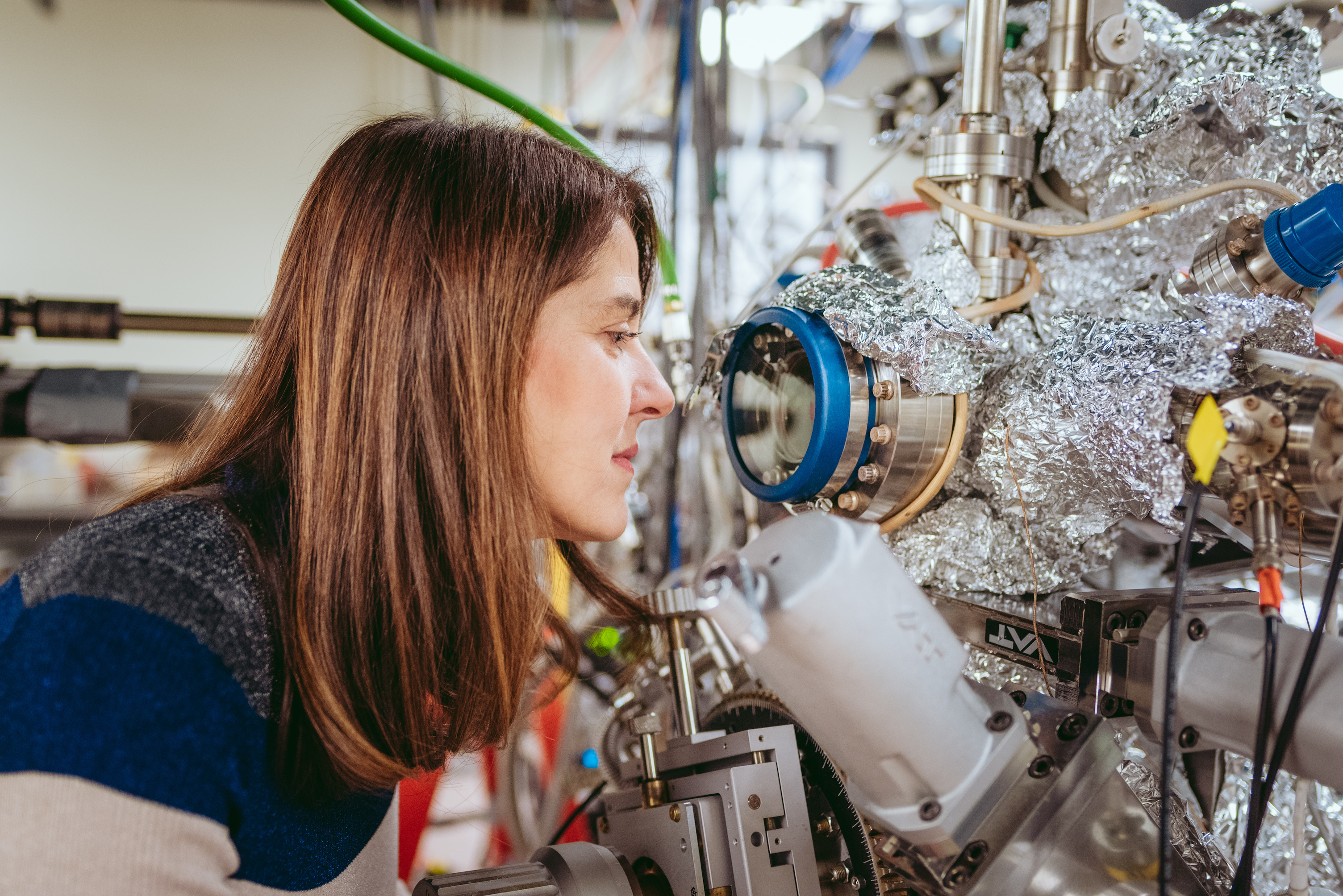
“Having access to higher resolution tools and new ways of probing materials is how we make new discoveries. It’s a must if you want to lead the way to new science.”
DEVELOPING NOVEL TOOLS
To build and investigate a diverse range of exotic 2D materials, Berkeley physicists are pioneering new techniques. “Having access to higher resolution tools and new ways of probing materials is how we make new discoveries. It’s a must if you want to lead the way to new science,” Lanzara says.
These experimentalists have favorite tools; for example, Wang specializes in studying how light interacts with materials.
“We use optical photons from near microwave to UV,” says Wang. “The combination of optical modalities depends on the material and the specific questions we’re trying to answer.”
Optical spectroscopy is Wang’s primary technique. But his group also uses scanning tunneling microscopy (STM), including a novel non-invasive spectroscopy technique he developed with Berkeley Physics Professors Alex Zettl and Michael Crommie.
Together they built a moiré superlattice from single layers of tungsten diselenide and tungsten disulfide and then added a spacer layer of boron nitride capped by a top layer of graphene. The graphene layer enabled them to sense a delicate crystal of electrons within the TMD moiré structure without destroying it with the STM tip. The spacer layer prevented electrical shorting and permitted independent doping for the TMD and graphene layers.
“We made the first real-space images of 2D Wigner crystals in our moiré superlattice by actually imaging a lattice formed by electrons. We were able to see the correlated ground state and interesting excited state properties,” Wang says.
This approach could also be used to image electron lattices in other materials, rather than relying on a “magic angle” between the layers to control the correlations. “Our TMD moiré superlattices exist even at zero twist angle due to the lattice mismatch, and the correlation effects remain strong,” says Wang.
Berkeley physicists are also directly measuring electrons and spin in momentum space using novel spin-, time-, and angle-resolved photoemission spectroscopy pioneered by Lanzara and her coworkers. In this technique, a material is irradiated with a beam of ultrafast photons and the spin, speed, and direction of the ejected photoelectrons are measured with incredible sensitivity to figure out what’s happening inside the material. Lanzara’s latest instrument, named the momentum nanoscope, can also look at real space.
Lanzara recently used her state-of-the-art system on the topological insulator bismuth telluride to search for novel types of excitons, which are charge-neutral quasiparticles created when light is absorbed in a semiconductor. Her team discovered and characterized the first spatially indirect topological exciton state. “The electron trapped on the surface is coupled to a hole confined in the bulk, generating a long-lasting spatially-separated exciton that retains the special spin properties inherent to topological states,” she says.
One potential application of exotic materials is sustainable electronics that stays cool. “Your cell phone and computer heat up because charges bounce into each other as they move,” explains Lanzara. “Some of these new 2D and topological materials allow information to be transported instead through spin, minimizing interactions and eliminating heating issues. Moreover, they can be combined as Lego-like blocks, enabling easy assembly of materials on demand that are reusable and recyclable.”
Just think, you might have an exotic 2D material in your pocket someday.
This is a reposting of my magazine feature, courtesy of UC Berkeley’s 2023 Berkeley Physics Magazine.
